Table of Contents >> Show >> Hide
- Why This Idea Matters Right Now
- What “Solderless, Soluble” Actually Means
- Material Stack: The Real Engine Behind the Idea
- How Solderless Assembly Changes the Engineering Workflow
- How Solubility Is Programmed (Not Left to Chance)
- What Real-World Research Has Already Proven
- Design Blueprint: Building a Practical Solderless, Soluble Board
- Challenges You Should Respect (Because Physics Has No Mercy)
- Where This Technology Is Headed
- Conclusion
- Extended Experiences (500+ Words): Lessons from Real Prototyping Practice
Let’s be honest: traditional circuit boards are amazing while they’re alive and mildly dramatic when they die.
They’re hard to disassemble, full of mixed materials, and often end up in a recycling limbo that looks more like a
junk drawer than a circular economy. Now imagine a different ending: a board that snaps together without solder,
performs its mission, and then safely dissolvesor is intentionally disassembled and recoveredwhen the job is done.
That is the core promise of a solderless, soluble circuit board.
This concept sits at the intersection of three fast-moving domains: solderless interconnects,
transient (dissolvable) electronics, and sustainable prototyping. The goal isn’t
to make every motherboard in your life vanish into a cup of water by Tuesday. The goal is smarter fit-for-purpose
hardware: medical implants that disappear after healing, temporary sensors that don’t require retrieval surgery,
and prototype boards that don’t become permanent landfill residents just because your first design had one resistor
in the wrong place.
In this guide, we’ll break down how a solderless, soluble PCB can work, where it already works, why it matters,
what still needs improvement, and how engineers can design one without turning the lab into a chemistry-themed escape room.
Why This Idea Matters Right Now
Electronics waste is still a major challenge. If your design cycle includes rapid prototyping, each iteration can produce
boards that are electrically useful for days but physically persistent for years. For one-off demos and short-duration tests,
this mismatch is expensive and wasteful.
At the same time, healthcare and wearable tech are pushing electronics into places where removal is risky, costly, or simply
unrealistic. Temporary implants are a perfect example: if a device is needed for one week, the body should not be asked to host
it indefinitelyor undergo a second procedure to remove it.
A soluble board architecture addresses both problems:
- Medical: Temporary operation, then bioresorption.
- Prototyping: Fast assembly/disassembly without heat damage from repeated soldering.
- Sustainability: Material recovery and lower end-of-life burden.
- Security: Potential for controlled physical disappearance of sensitive hardware.
What “Solderless, Soluble” Actually Means
Solderless
Solderless doesn’t mean “magic.” It means the electrical and mechanical connections are created without melting solder alloy.
Common options include:
- Press-fit or compliant pins inserted into plated-through holes.
- Spring contacts, pogo pins, and socketed modules.
- Conductive adhesives (for low-temperature joining where heat is undesirable).
- Plug-and-play terminal strips like breadboard-style architectures for rapid iteration.
Soluble
Soluble means the board (or defined parts of it) can physically break down in a controlled environmentwater, biofluids, or
triggered conditionsinto components that are either biocompatible, benign, or recoverable. “Soluble” is not the same as
“instantly gone.” Smart transient electronics are tuned for a useful service window and a planned end-of-life pathway.
Material Stack: The Real Engine Behind the Idea
1) Substrates That Can Disappear
Conventional FR-4 is robust, cheap, and stubbornly permanent. Soluble alternatives depend on use case:
- Biomedical transient systems: bioresorbable polymers and ultrathin films engineered for hydrolysis.
- Prototype recycling boards: water-soluble polymers such as PVA-based substrates.
- Hybrid architectures: non-soluble structural frame + soluble functional layer for selective recovery.
The smart move is not “make everything dissolve,” but “make the right layer dissolve at the right time.”
2) Conductors That Can Be Recovered or Resorbed
Conductive traces in dissolvable systems may use ultrathin metal films, patterned transient conductors, or liquid-metal-inspired
designs in prototyping contexts. In some cases, the substrate dissolves while the conductor is physically recovered and reused.
This is ideal for iterative design workflows where conductor material cost and waste both matter.
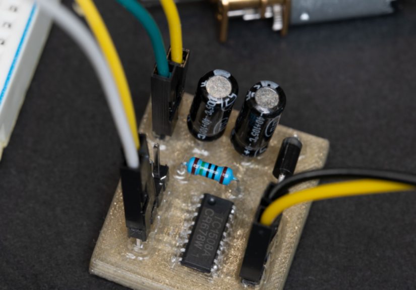
3) Component Strategy
Here’s the practical truth: full-soluble integrated circuits are still specialized. So many near-term designs use a
split architecture:
- Disposable or soluble base platform
- Removable high-value components (MCUs, sensors, radios) on sockets or reusable daughterboards
- Solderless interconnects for quick swap and minimal thermal stress
Think of it like a stage set: the scenery is temporary, the lead actors return for the next show.
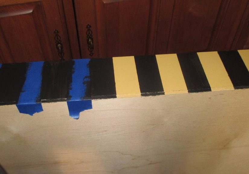
How Solderless Assembly Changes the Engineering Workflow
Faster Iteration and Rework
In classic prototyping, one wrong footprint can trigger a solder wick marathon. Solderless layouts dramatically reduce rework time.
You can swap modules, tune signal paths, and test alternatives without cooking pads or delaminating fragile substrates.
Lower Thermal Load
Soluble and bioresorbable materials can be heat-sensitive. By minimizing high-temperature reflow, solderless joining preserves
mechanical integrity and expands material options.
Mechanical Design Becomes First-Class
With press-fit, clips, and compliant contacts, mechanical tolerances are no longer an afterthought. Hole geometry, insertion force,
surface finish, and cycling durability become critical to reliable conductivity.
How Solubility Is Programmed (Not Left to Chance)
Time-Based Dissolution
Engineers tune device lifetime using thickness, encapsulation strategy, material chemistry, and exposed surface area.
Example: a sensor may remain stable through a known post-op window, then gradually resorb.
Trigger-Based Dissolution
Some systems use specific triggersmoisture ingress, temperature conditions, or externally activated eventsto start degradation.
This is especially relevant for temporary security hardware and environmental sensing missions.
Selective Dissolution
A board can be designed to lose only certain functions first (e.g., communication layer), while core data storage remains inaccessible,
or vice versa. This allows nuanced end-of-life behavior beyond all-or-nothing “melt mode.”
What Real-World Research Has Already Proven
The field is no longer hypothetical. Early landmark university work established bioresorbable circuits that dissolve after completing
medical tasks. Since then, researchers have demonstrated temporary neural and physiological monitoring platforms, wireless transient
pacemakers, and eco-focused recyclable prototyping boards.
Notable advances include:
- Transient biomedical sensors: Devices that monitor pressure and temperature for clinically relevant windows,
then dissolveremoving the need for extraction procedures. - Wireless dissolvable pacing systems: Temporary pacemakers designed for short-term cardiac support and natural
disappearance after use. - Soluble prototyping PCBs: Water-soluble substrate approaches that allow high material recovery for rapid board iteration.
If this sounds futuristic, it is. If it sounds impossible, it isn’t.
Design Blueprint: Building a Practical Solderless, Soluble Board
Step 1: Define the Mission Lifetime
Start with duration, not materials. Is your device needed for 6 hours, 7 days, or 6 weeks? Lifetime defines everything: encapsulation,
interconnect choice, protection strategy, and testing protocol.
Step 2: Partition the System
Separate into:
- Ephemeral layer: substrate and low-cost passive network
- Recoverable core: expensive active components in sockets or modules
- Interconnect bridge: solderless contacts or conductive adhesive paths
Step 3: Choose Connection Strategy by Electrical Class
- Low-speed digital / sensing: spring contacts, socket blocks, conductive adhesives
- Higher-current paths: robust press-fit/terminal options with validated insertion mechanics
- RF/precision analog: keep paths short, impedance-aware, and mechanically stabilized
Step 4: Plan End-of-Life Upfront
Decide whether your board should:
- Fully dissolve in a controlled medium
- Dissolve substrate while recovering conductor/materials
- Disassemble into reusable modules and recyclable disposables
“We’ll think about disposal later” is how good prototypes become bad waste.
Step 5: Test for the Entire Lifecycle
Validation should include:
- Electrical stability over intended use window
- Mechanical cycling of solderless contacts
- Dissolution behavior under realistic media and temperature conditions
- Residue/toxicity profile (especially for biomedical use)
- Recovery efficiency for reusable materials
Challenges You Should Respect (Because Physics Has No Mercy)
Contact Reliability
Solderless interfaces can drift in resistance with vibration, oxidation, or poor insertion geometry. Design margins, contact finish,
and retention mechanics are non-negotiable.
Moisture vs. Lifetime Control
If the board dissolves too early, it fails in service. Too late, it fails sustainability. Encapsulation engineering is the art of
controlled timing.
Component Compatibility
Not every off-the-shelf IC is happy in transient packaging environments. Hybrid modular design is currently the most realistic path for
many commercial teams.
Regulatory Requirements
Medical applications must satisfy rigorous biocompatibility and risk-based evaluation standards. “It dissolved in a beaker” is not a
substitute for clinical-grade evidence.
Where This Technology Is Headed
Over the next few years, the most likely growth zones are:
- Post-operative temporary implants (monitoring, stimulation, localized therapy)
- Sustainable education and maker platforms for low-waste hardware learning
- Short-term industrial/environmental sensing where retrieval is expensive
- Secure electronics with controlled physical end-of-life behavior
In parallel, manufacturing research will continue improving low-temperature interconnects, dissolvable substrates, and circular recovery
pathways. The big win will come when performance, reliability, and sustainability are designed as one systemnot three separate afterthoughts.
Conclusion
A solderless, soluble circuit board is not a gimmick. It is a new design philosophy for electronics that are temporary by intent and
responsible by default. Instead of forcing every device into the “forever hardware” model, engineers can now choose lifecycles that match
real mission needs.
The practical path forward is clear: use solderless modular architecture for speed and reuse, apply soluble materials where temporary
function is enough, and engineer end-of-life behavior as carefully as startup behavior. In short: build boards that do their job, then
exit gracefullyno drama, no landfill monologue, no encore.
Extended Experiences (500+ Words): Lessons from Real Prototyping Practice
The most useful lesson I’ve seen in teams exploring solderless, soluble boards is this: success starts with admitting that you are not
designing a “normal PCB with greener branding.” You are designing a lifecycle. In one early prototype sprint, a team copied a conventional
layout strategy, swapped in a water-soluble substrate, and expected similar reliability. The board worked perfectly for about two hours,
then contact resistance rose in unpredictable places. Why? The layout assumed the same mechanical stability as rigid FR-4, but the new
substrate flexed under cable strain and humidity. The fix was not electrical firstit was mechanical. We added strain-relief geometry,
changed connector placement, and shifted to shorter signal loops near critical sensors. Electrical performance stabilized immediately.
Another recurring insight: solderless does not mean careless. People hear “plug-and-play” and imagine infinite connector swaps without
consequences. In reality, insertion cycles matter. Contact surfaces age. Oxidation appears. Minor misalignment can become major noise.
A strong team habit is to treat each reconfiguration like a controlled experiment: log the cycle count, measure key node resistances,
and check baseline drift before and after every major hardware change. This discipline feels boring until it saves a week of debugging.
On the soluble side, dissolution testing taught us humility. A board that dissolved in 20 minutes in static lab water survived far longer
in low-flow fluid with different ionic conditions. Another board did the opposite. The takeaway: always test in realistic environments.
If your target is a medical window, bench chemistry alone won’t represent physiology. If your target is maker-space recycling, tap water
variability and temperature swings can change the result more than expected. Teams that define a “dissolution envelope” (best case, nominal,
worst case) produce designs that behave predictably outside perfect demos.
One project that worked especially well used a two-tier architecture. The disposable board handled routing, passives, and temporary
connectors; a tiny reusable compute module snapped in through a robust mechanical interface. At end-of-life, the substrate dissolved,
conductors were recovered, and the expensive module was redeployed. Economically, this mattered as much as sustainability. Engineers were
more willing to iterate because each design mistake no longer destroyed the costly parts.
There were also user-experience surprises. Non-electrical team membersindustrial designers, clinicians, field testerswere much more
willing to participate when the board could be assembled and modified without soldering stations. That changed collaboration speed. A nurse
could request a lead repositioning and see a physical revision in the same session. A product designer could test curved placement options
without waiting for a new reflow cycle. In other words, solderless architecture didn’t just change manufacturing; it changed who could
contribute meaningfully to hardware decisions.
The biggest long-term lesson is philosophical: “temporary” should never mean “fragile and approximate.” The best soluble, solderless systems
are engineered with the same rigor as permanent electronicsjust with a smarter ending. They have clear performance budgets, defined operating
windows, validated interconnect mechanics, and explicit retirement pathways. Teams that embrace this mindset stop asking, “Can we make it
dissolve?” and start asking, “Can we make it perform flawlessly until it dissolves?” That question produces better science, better
products, and better stewardship of materials.