
Table of Contents >> Show >> Hide
- What Is a Printed Circuit Board, Exactly?
- Step 1: Define the Circuit Before You Touch the Layout
- Step 2: Choose Components and Match Them to Footprints
- Step 3: Plan the Board Layout Like a Strategist, Not a Gambler
- Step 4: Run Design Rule Checks and Manufacturability Reviews
- Step 5: Generate the Manufacturing Files
- Step 6: Prototype, Assemble, Test, and Improve
- Should You Make a PCB at Home or Use a Professional Fabricator?
- Common PCB Design Mistakes to Avoid
- Best Tools for Creating Printed Circuit Boards
- Real-World Examples of Simple First PCB Projects
- Experience-Based Lessons From Creating Printed Circuit Boards
- Conclusion
- SEO Tags
If you have ever looked at a tangled breadboard and thought, “There has to be a less spaghetti-shaped way to do this,” welcome to the wonderful world of printed circuit boards. A PCB is what turns a loose collection of electronic parts into something sturdy, repeatable, and far less likely to fall apart the moment someone sneezes near it. From simple LED blinkers to compact sensor modules and custom controllers, PCBs are the bridge between an idea and a real product.
Creating a printed circuit board is not just about drawing a few lines and clicking “order.” A good board starts with a smart schematic, moves through careful layout, survives design rule checks, and ends with manufacturing files that a fabricator can actually use without sending you an email that begins with, “So… what exactly did you mean here?” The good news is that the process is more approachable than ever. Modern CAD tools, better tutorials, and low-cost fabrication services have made PCB design much easier for beginners and much faster for experienced builders.
In this guide, you will learn how to create printed circuit boards step by step, what decisions matter most, which mistakes show up again and again, and how to move from concept to finished board without losing your mind or your copper. We will focus mostly on the modern workflow for professionally fabricated boards, because it is cleaner, more accurate, and much more web-publishable than a chemistry experiment gone rogue on the kitchen table.
What Is a Printed Circuit Board, Exactly?
A printed circuit board is a flat board made from insulating material with conductive copper traces that connect electronic components. Depending on the design, it may have one layer, two layers, or multiple layers of copper. Most beginner and hobbyist boards are one-layer or two-layer boards, while more advanced designs often use four or more layers for better power delivery, signal routing, and noise control.
In plain English, a PCB does three big jobs. First, it provides electrical connections between parts. Second, it gives those parts mechanical support. Third, it makes the whole circuit easier to build, test, reproduce, and improve. That is why nearly every modern electronic device relies on one.
Step 1: Define the Circuit Before You Touch the Layout
The first step in creating a PCB is not drawing the board outline. It is defining the actual circuit. Start with a clear goal. Are you building a small Arduino shield, a USB-powered sensor board, a motor driver, or a power supply module? Your answer affects everything that follows, including board size, connector choice, trace width, heat handling, and how many layers you may need.
Once the function is clear, create a schematic in your EDA software. This is the logical diagram that shows how the components connect. A clean schematic saves time later because it helps you catch bad pin assignments, missing pull-up resistors, backwards diodes, and the kind of mistakes that only become expensive after you have already ordered ten boards.
At this stage, choose real parts, not vague placeholders. Instead of writing “some capacitor, probably,” pick an actual value, package, and part type. Instead of “a connector,” decide whether you need USB-C, screw terminals, pin headers, or JST connectors. Real design starts when the components stop being imaginary.
Helpful Tip
If this is your first board, keep the project modest. A simple LED driver, sensor breakout, or button-and-buzzer board will teach you more than a heroic ten-hour attempt to build a four-layer Wi-Fi gadget with no sleep and excessive confidence.
Step 2: Choose Components and Match Them to Footprints
After the schematic comes one of the most important parts of PCB design: matching every schematic symbol to the correct PCB footprint. This is where the virtual design meets physical reality. If the footprint is wrong, the board may look beautiful on screen and still be completely useless in the real world.
A footprint defines the copper pads, hole sizes, spacing, and placement for a component. Through-hole parts are generally easier for beginners to solder by hand. Surface-mount parts save space and are standard in modern electronics, but they can be more challenging if you choose tiny packages too early. For a first design, avoid microscopic components unless you enjoy soldering with the emotional intensity of bomb disposal.
Double-check the following before moving on:
- Pin numbering and orientation
- Package type, such as SOIC, QFN, 0805, or THT
- Hole sizes for through-hole parts
- Connector dimensions and mechanical fit
- Manufacturer datasheet recommendations
Step 3: Plan the Board Layout Like a Strategist, Not a Gambler
Now the fun part begins. PCB layout is where you place components on the board and route copper traces between them. It is also where many beginners discover that electronics is not only science. It is geometry, planning, and occasionally mild emotional turbulence.
Start by drawing the board outline. Then place the biggest and most important parts first. Connectors, mounting holes, switches, displays, and power inputs should usually be placed before small resistors and capacitors. Think about how a real person will use the board. Where will cables go? Where will screws go? Which side needs clearance? Which parts get hot? A PCB is not just an electrical drawing. It is a physical object that must exist in three-dimensional reality, where bad decisions are less theoretical.
Next, group related components together. Decoupling capacitors should sit close to IC power pins. Power circuitry should stay logically arranged. Sensitive analog sections should not be tossed beside noisy switching sections like they are roommates who will “figure it out.” Good placement often makes routing dramatically easier.
Layout Best Practices
- Keep traces as short and direct as practical
- Use wider traces for higher current paths
- Keep return paths and ground strategy in mind
- Avoid awkward routing that creates unnecessary loops
- Leave enough spacing for manufacturing and soldering
- Use ground pours where appropriate, especially on two-layer boards
If your design is more complex, consider stack-up and signal integrity earlier rather than later. A simple two-layer board is fine for many projects, but fast digital signals, RF sections, dense microcontrollers, and power-sensitive layouts may benefit from four layers or more. More layers usually mean better routing options and cleaner power distribution, though they also add cost.
Step 4: Run Design Rule Checks and Manufacturability Reviews
Before you generate manufacturing files, run your design rule check, also called DRC. This verifies that trace width, clearance, drill sizes, annular rings, and board-edge spacing meet your fabrication service’s limits. In other words, it answers a very important question: can this board actually be built, or is it just aggressively optimistic artwork?
Different PCB fabricators have different capabilities, so always review their rules before finalizing the design. A board that works with one manufacturer’s limits may fail with another’s. This is especially important for narrow traces, tight spacing, tiny drill holes, slots, cutouts, and unusual board shapes.
You should also perform a design-for-manufacturing review. Check pad sizes, verify part orientation, confirm polarized parts, inspect silkscreen readability, and make sure test points and labels are sensible. If the board will be assembled professionally, verify that the bill of materials, reference designators, and placement data are ready and consistent.
Things to Check Before Ordering
- Every component has a valid footprint
- No traces are too thin for their current load
- No copper is too close to the board edge
- Mounting holes and cutouts are correctly defined
- Silkscreen is not printed over pads
- Board dimensions match the enclosure, if there is one
- Polarized parts are clearly marked
- Connector orientation makes real-world sense
Step 5: Generate the Manufacturing Files
Once the layout is complete and the checks pass, generate the files your manufacturer needs. The most common outputs are Gerber files for each board layer and NC drill files for the holes. These files tell the fabrication house what copper to keep, where to drill, what layers exist, and how the board outline should be cut.
If your design tool offers a manufacturing preview, use it. A visual inspection of the final output can catch errors that a DRC may miss, such as missing layers, wrong board outlines, or mirrored text. Think of it as the “read your own text before hitting send” phase of PCB design.
You may also need:
- A bill of materials for assembly
- Pick-and-place files for automated assembly
- Fab notes or special instructions
- Stack-up information for multilayer boards
- Panelization details for production runs
For simple prototypes, many designers upload Gerbers directly to a board house, choose thickness, copper weight, solder mask color, and quantity, then place the order. For higher-volume or more demanding designs, communication with the fabricator becomes much more important.
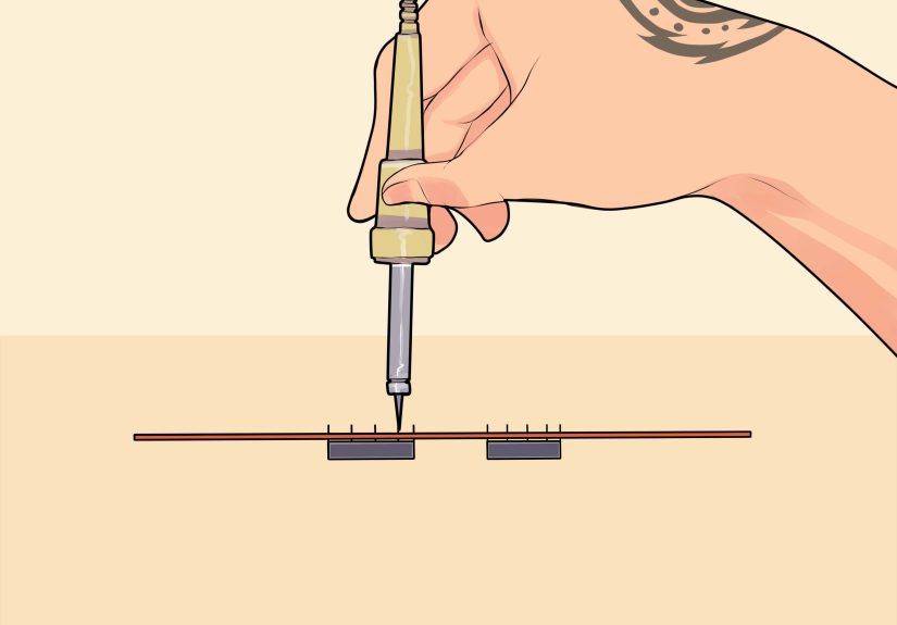
Step 6: Prototype, Assemble, Test, and Improve
The first PCB version is rarely perfect, and that is normal. Prototyping is where theory meets reality, and reality tends to have opinions. Once the boards arrive, inspect them carefully before assembly. Look for broken traces, solder mask issues, damaged edges, wrong hole sizes, or anything else suspicious.
Then assemble the board. If you are hand-soldering, start with low-profile components and work up to taller parts. If you are using surface-mount components, practice on simpler packages before moving to fine-pitch parts. After assembly, do not plug the board into your expensive equipment immediately like a person who enjoys surprise smoke. First, check for shorts, verify continuity on critical nets, inspect solder joints, and confirm the power rails with a multimeter.
Testing should be structured, not random. Power the board in stages if possible. Validate regulators first. Then check clocks, interfaces, LEDs, buttons, sensor readings, and communication links. A methodical test plan makes debugging faster and less dramatic.
Should You Make a PCB at Home or Use a Professional Fabricator?
Technically, both are possible. Practically, professional fabrication is the better option for most modern projects. Home-made PCBs can still be useful for learning, rough one-off experiments, or purely educational demonstrations. However, professionally fabricated boards usually provide better trace accuracy, plated holes, solder mask, silkscreen, tighter tolerances, and cleaner results overall.
Home methods also come with mess, safety concerns, and a much lower tolerance for tiny mistakes. That is why most makers and engineers now design the board digitally and send the manufacturing files to a fabrication service. It is often cheaper than expected, and it saves an enormous amount of time.
Common PCB Design Mistakes to Avoid
- Using the wrong footprint: the classic mistake that turns a real board into decorative electronics art.
- Ignoring current requirements: high-current traces need enough width and proper thermal thinking.
- Poor component placement: bad placement makes routing harder and performance worse.
- Weak grounding strategy: noisy layouts often start with careless ground planning.
- Skipping DRC: this is like refusing to proofread a legal document written in permanent ink.
- No test points: debugging becomes much more painful when you cannot probe important signals.
- Forgetting mechanics: connectors, enclosures, and mounting holes are not optional afterthoughts.
Best Tools for Creating Printed Circuit Boards
Many designers use tools such as Autodesk Fusion Electronics, Cadence tools, EasyEDA, KiCad, or other PCB CAD platforms. The right choice depends on your budget, experience, collaboration needs, and manufacturing workflow. A beginner-friendly interface is great, but the most important thing is learning the underlying design process: schematic capture, footprint verification, layout, rule checking, and manufacturing output. Software changes. Good habits travel.
Real-World Examples of Simple First PCB Projects
If you want practical ideas, here are excellent first-project categories:
- A custom LED flasher board
- A sensor breakout for temperature, motion, or light
- A USB-powered microcontroller carrier
- A button-and-buzzer training board
- A small relay or MOSFET driver board
These projects are simple enough to learn from, yet rich enough to teach real PCB skills: connector choice, decoupling, trace routing, labels, and assembly planning.
Experience-Based Lessons From Creating Printed Circuit Boards
One of the most common real-world experiences in PCB design is discovering that the board was never really the problem. The footprint was. A designer can spend hours rerouting traces, moving components, and polishing silkscreen, only to realize that a connector footprint is mirrored or an IC package is off by one pin. That is why experienced designers become borderline obsessive about datasheets. They know a five-minute footprint review can save a two-week ordering delay.
Another common lesson is that placement solves more problems than routing. Beginners often dive straight into traces because it feels productive. Experienced designers pause longer. They nudge a regulator closer to a connector, rotate an IC by ninety degrees, move decoupling capacitors tighter to power pins, and suddenly the routing becomes cleaner. It is one of those satisfying engineering moments where everything improves because one early decision got smarter.
There is also the surprisingly emotional experience of receiving your first manufactured PCB. On screen, it looked like lines and labels. In your hand, it feels like proof that an idea crossed the border into reality. Even when revision one is imperfect, it teaches lessons fast. Maybe the USB port collides with the enclosure. Maybe the button is too close to a mounting hole. Maybe the status LED is hidden behind a connector because someone, not naming names, thought three-dimensional access was a future problem. That first board is a strict but excellent teacher.
Debugging prototypes creates its own set of unforgettable moments. Sometimes the board powers up immediately and behaves like a polite little genius. More often, it sits there in silence while you check voltages with the expression of a detective in a low-budget mystery. Then you find it: a missing pull-up, a swapped TX and RX line, a ground pour that did not connect the way you assumed, or a net label that looked right until you actually read it carefully. PCB design has a funny way of rewarding patience more than ego.
Another experience many engineers mention is how quickly manufacturability becomes part of design thinking. Early on, it is easy to think only in terms of electrical function. Later, you start asking better questions. Can this be assembled easily? Is there enough room for a soldering iron? Will a technician be able to probe this signal? Is the silkscreen readable after the connectors are installed? Can the board survive handling, heat, and repeated use? These questions turn a circuit into a product.
Perhaps the biggest long-term lesson is that PCB design is iterative by nature. Strong boards are rarely born perfect. They are refined through prototype cycles, testing, notes, and small corrections that stack up into quality. The best designers are not the ones who never make mistakes. They are the ones who build systems that catch mistakes early, learn from every revision, and improve without drama. In that sense, creating printed circuit boards is part engineering, part craftsmanship, and part humility training with copper attached.
Conclusion
Learning how to create printed circuit boards is one of the most useful skills in electronics. It turns fragile prototypes into reliable hardware, makes troubleshooting more structured, and gives you far more control over how a project looks, works, and scales. The basic workflow is straightforward: define the circuit, choose real components, match correct footprints, place parts intelligently, route with care, run design checks, generate manufacturing files, then prototype and test.
The biggest secret is that good PCB design is not about fancy software tricks. It is about thoughtful decisions. If you focus on clarity, manufacturability, and practical testing, your boards will improve quickly. And when your first successful PCB arrives in the mail, you will understand why so many electronics people become mildly obsessed with tiny green rectangles.